back to competences
We offer various wafer-scale technologies in-house. From patterning, jetting, and machining to wafer bonding and dicing. All to create packages where active components (VCSEL, LED) can be combined even with integrated apertures and replicated optics.
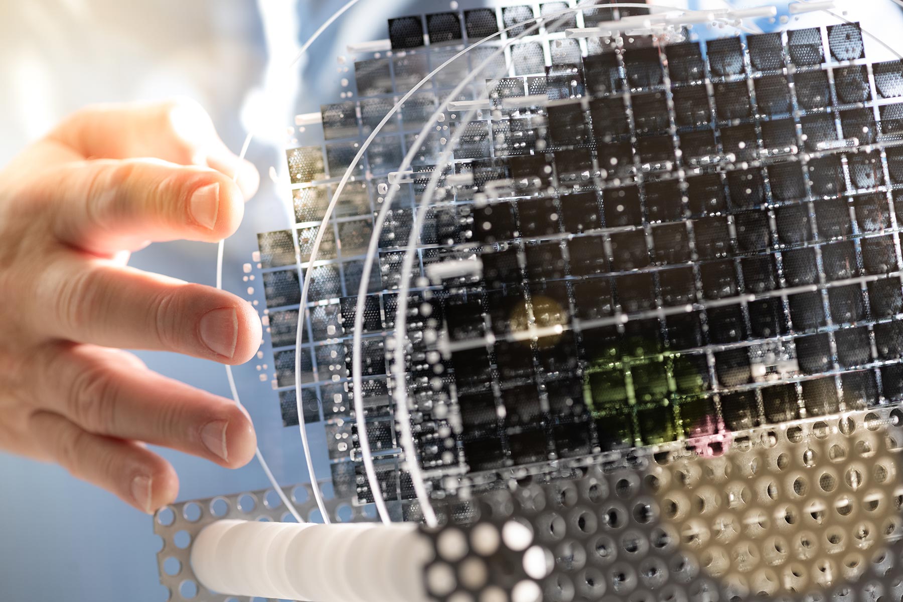
Trends toward miniaturization and cost-effectiveness require the integration of active opto-electric components into custom packages.
Various wafer scale technologies such as metal coating and patterning to create electrical traces, micro jetting for die attach, powder blasting or laser machining for via creation, wafer bonding and dicing are available to create opto-electronic packages where active optical components can be combined even with integrated apertures and replicated optics.